PCB Manufacturing

Propelling Rapid, Low Cost 24/7 PCB Production

Spectra-Physics is a leading supplier of lasers for the manufacture of printed circuit boards and microelectronics packaging. Our lasers are proven in a wide range of PCB applications including cutting, depaneling, via hole drilling, direct imaging, trimming, repair and marking. With thousands of lasers deployed in demanding PCB applications, Spectra-Physics delivers a broad portfolio of highly reliable, cost-effective lasers backed by our industry-leading global support organization.

  • Powering critical PCB apps: cutting, drilling, LDI, trimming, repair, marking etc.
  • Proven in demanding volume production
  • Driving highest throughput
  • Delivering disruptive cost-performance

PCB Cutting and Via Drilling

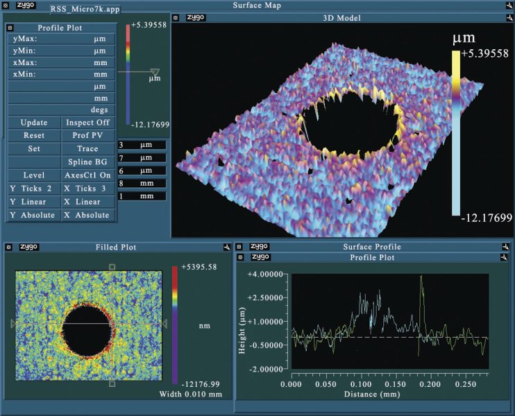
As electronic devices shrink and improve in performance, the need for compact and thin flex-PCBs to which the electronic devices are mounted is growing rapidly. Flex-PCBs are typically made using layers of materials that have several to tens of .m thicknesses. Materials used include copper (Cu) foils, polyimide (PI) sheets, and adhesives that enable the creation of various laminates. A typical flex-PCB material is comprised of a 12 μm thick PI layer laminated between two Cu foils of similar thickness. In flex-PCB fabrication, laser processes may include blind- and thru-via drilling, straight-line and contoured cutting, as well as 2D patterning. Please see Newport.com for additional information on PCB Manufacturing.

Profile of a via hole drilled in flex-PCB using a Spectra-Physics Talon UV ns laser
Figure 1. Profile of a via hole drilled in flex-PCB using a Spectra-Physics Talon UV ns laser. The flex-PCB layer is a Cu/PI/Cu laminate. The via hole was trepan cut with an 80 .m diameter. The resulting average burr height was < 2 μm..

PCB Manufacturing Lasers

Application Notes

Cutting and Drilling of PCB Materials

Precision micromachining achievable with UV lasers allows more circuits to fit on a single panel, increasing the net usable area. Moreover, UV wavelengths are absorbed by a variety of materials in PCBs, from copper to polyimide films, thus providing a onesolution-for-all-materials-and-processes kind of flexibility. For example, the high beam intensity achievable with tighter focus UV can remove copper, while lower beam intensity achieved by reducing laser power can cut dielectric material without damaging the bottom copper layer. See Cutting and Drilling of PCB Materials Using UV Talon® Laser for additional information.

Fast Flex-PCB Processing

For industrial OEM manufacturing, Spectra-Physics introduced Talon®, a disruptive cost-performance line of UV lasers. One large and growing market for laser processing is PCB manufacturing, which has traditionally used CO2 and excimer lasers but is increasingly moving towards UV DPSS lasers. The migration to UV DPSS laser technology isdriven by several factors, including the need to machine smaller features with higher precision and density, the ability of UV wavelengths to process many types of materials with good quality and the improving cost-performance of UV DPSS products available on the marketplace. See High Power, High Repetition Rate UV Lasers for Fast Flex-PCB Processing  for additional information.